 HackerTube.runGood videos, with context.
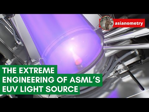
The Extreme Engineering of ASML’s EUV Light Source
About this video
Asianometry explains the EUV light source inside ASML's lithography machines, where lasers hit falling tin droplets twice to produce 13.5 nm light. It walks through the engineering of the droplet generator, the pre-pulse and main laser, and the plasma that results.
Why it appears in the archive
Commenters repeatedly point to it whenever EUV, ASML or chip manufacturing comes up, as a clear and astonishing explanation of one of the hardest engineering problems in chipmaking.
AI-generated summary and labels from the source dataset; verify important details against the video. Source & credits.
From the Hacker News discussion
Because the EUV machines that ASML build are the most complex machines ever built by humans and getting all the bits to work properly takes decades of R+D e.g. watch this about the light source, its completely bonkers [VIDEO]
Read original comment ↗EUV lithography is interesting. You drop a microscopic droplet of tin. You then aim and shoot it not once, but twice with a laser so it produces the correct wavelength. Then you do this with 100% reliability thousands of times per second all day, every day for years. The problem doing this with fusion seems to be money. Their "big" grant of 600M wouldn't even buy a handful of those machines and wouldn't come close to the many billions it has cost in the past 30+ years of research to reach the point where they are finally viable (it had been "a few months away" ever since the early 2000s). This video from Asianometry on EUV light sources is well worth the watch. It's pretty incredible. [VIDEO]
Read original comment ↗Anyone interested in the details should watch this video: [VIDEO] (has the same graphics) without any hyperbole the 2-shot laser thing necessary to emit EUV is just mind bending.
Read original comment ↗Two must watch videos about the whole process: [VIDEO] [LINK] (Typed on a device made by this process, which I still don’t quite believe.)
Read original comment ↗To add to this, here is a great video on some of the technical/physical challenges ASML had to solve for their EUV source: [VIDEO]
Read original comment ↗Cant answer the question and my knowledge is only from 'one interested' but from how long (~20 years) it took to build the current EUV source and how complicated the alternatives look this is for sure no easy feat. Can recommend [1] as the title say about the light source. Very interesting even for a non professional (and [2] as on high level overview of the machine and [3] as longer documentation inside ASML). [1] [VIDEO] "The Extreme Engineering of ASML’s EUV Light Source" [2] [LINK] "The Extreme Physics Pushing Moore’s Law to the Next Level" [3] [LINK] "ASML's Secret: An exclusive view from inside the global semiconductor giant"
Read original comment ↗The machines are made by other companies. Lithography is the most expensive now and its made by ASML in Netherlands is the only solution for EUV lithography. But there are many steps in manufacturing and a machine for each. The major equipment manufactures are spread across US, Europe and Japan. In the US the three big equipment manufacturers are Applied Materials and Lam Research and KLA. The costs are probably driven by extreme engineering requirements (temperature, pressure, corrosive chemicals, low contamination) and R&D costs to meet these requirements. The production volumes are not high either. Its not like they are building millions of these machines. Asianometry on YouTube is a good source for this kind of topic. [VIDEO]
Read original comment ↗The etching process that uses a laser to blast a moving molten tin sphere to shape it so the next laser blast that vaporizes it produces parallel EUV light is pretty insane, too. See [VIDEO]
Read original comment ↗