 HackerTube.runGood videos, with context.
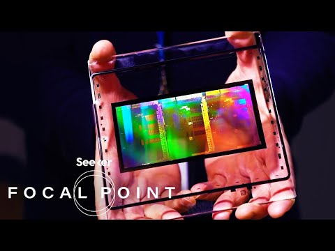
The Extreme Physics Pushing Moore’s Law to the Next Level
About this video
Seeker's Focal Point short documentary on ASML's extreme ultraviolet lithography machines, which make the most advanced chips. It shows how plasma-generated 13.5 nm light is used to push Moore's Law forward.
Why it appears in the archive
HN links it in semiconductor threads as an accessible overview of why EUV lithography is so hard.
AI-generated summary and labels from the source dataset; verify important details against the video. Source & credits.
From the Hacker News discussion
I don't understand callous contempful comments against Intel's manufacturing capabilities. There are incredible people making things possible fomr both sides in one of the most advanced manufacturing processes in the world. I've worked inside a fab and I can tell you that the industry is much more appreciative of each other's competitors than the outside fanboys who are largely pissed off at the executive decisions (lawsuits , etc). This article is about TSMC's technical achievements and your comment has not added anything to the discussion, time and again I see this rooting for "underdog" behavior all too the same (just flipped the sides) from 2006. I wrote about it here: [LINK] If you'd like to know what goes into shriking a process node from lithography standpoint, I implore you to watch this: [VIDEO] and be in complete utter awe... Tell me if they are "Sitting on their asses"?
Read original comment ↗Seeker released a very insightful feature about the ASML Extreme UV / soft X-ray (13.5 nanometers) photolithography system that is being referred to in the article. [VIDEO]
Read original comment ↗I think the culture is improving despite of cashing it out in the 90's and 2000's during the Ballmer / Jack Welsch era. Semiconductor industry hasn't done a good job of cultivating a good, positive company culture and making it less regimented. We need to make it cool to work in a semiconductor company. I can assure you that there are so many incredible challenges that exist - with good definition/funding to tackle them from materials to marketing (direly needs to revamped). Imagine running a portion of the world's most advanced manufacturing processes. Ultra high volume (thousands of wafer starts per week), mind you. Perhaps videos such as these are shining a positive light on the entire semiconductor goodwill: [VIDEO]
Read original comment ↗This was also a cool video I saw recently about lithography with plasma lasers [VIDEO] around 7:14 in particular
Read original comment ↗Each additional step requires solving a lot of new engineering problems and usually some new physics too, and it's not a linear process: many techniques are proposed that become cost effective only when previous techniques hit their size limits, and then a lot of research is done and most techniques are never gotten to work at scale and just a few pan out and become the next process. This is a great talk on the history of chip processes: [LINK] This is about some of the challenges that had to be solved for a current modern process: [VIDEO]
Read original comment ↗Cant answer the question and my knowledge is only from 'one interested' but from how long (~20 years) it took to build the current EUV source and how complicated the alternatives look this is for sure no easy feat. Can recommend [1] as the title say about the light source. Very interesting even for a non professional (and [2] as on high level overview of the machine and [3] as longer documentation inside ASML). [1] [LINK] "The Extreme Engineering of ASML’s EUV Light Source" [2] [VIDEO] "The Extreme Physics Pushing Moore’s Law to the Next Level" [3] [LINK] "ASML's Secret: An exclusive view from inside the global semiconductor giant"
Read original comment ↗The entire world has their eggs in one basket - Taiwan Semiconductor Manufacturing Company. Say whatever about Intel, I am hoping that they get back on their feet in next few years with 5nm manufacturing. Since when is competition and choice a bad thing? If you're a chip design firm and you have a 8-month backlog to get your masks made at TSMC, what do you do then? TSMC can be world's best fab but we need to address the SPOF condition that is so close to the political hot zone in the APEC region. Intel should spin off its Fab division as a separate company, hire some top executives to rejuvinate the workforce, make it the coolest Fab company in the world to work for and leap ahead. Intel TMG's Sohail was the biggest borderline criminal executive that was forced out a couple of years ago and was responsible for the 10nm delays. It is enormously difficult for any startup to get into this space - you need billions and years of expertise to start a Fab. Or may be YC folks can? I worked in the Fab but don't have a birds-eye view of what it takes for a startup to get into this space. It would be amazing to see startups trying to manufacture semiconductors... you know live up to the Silicon Valley's name. You could have billions of dollars of economy built on services - US, EU and most advanced economies are shifting towards services; but they all rely on semiconductors. Imagine something were to happen to that... It is a juicy problem. We don't need Uber/AirBnb unicorns out of SV,
Read original comment ↗Worth mentioning is the insane and disruptive technology making TSMC's 5nm possible. ASML and it's suppliers have built a machine[1] that has a sci-fi feel to it. It took decades to get it all right, from the continous laser source to the projection optics for the extreme ultraviolet light[2]. This allowed photolithography to jump from 193nm light to 13.5nm, very close to x-rays. The CO2 laser powering the EUV light source is made by Trumpf[3]. Edit:More hands-on video from Engadget about EUV at Intels Oregon facility[4] [1] [LINK] [2] [VIDEO] [3] [LINK] [4] [LINK]
Read original comment ↗